+86 135 3053 5995
sales@mydled.comWe use our own and third-party cookies to ensure the proper functioning of the web portal and its complements, perform navigation analysis and show multimedia content. If you continue browsing, you accept the use of this technology. For more information please see our Cookies Policy. Learn more
LED components account for about 40% to 70% of LED display costs, and the significant reduction in LED display costs is due to the lower cost of LED components. The quality of the LED package has a great impact on the quality of the LED display. The key to package reliability includes the choice of chip materials, the choice of packaging materials and process control. In addition, strict reliability standards are key to testing high quality LED components.
As LED displays gradually develop toward the high-end market, the quality requirements for LED display components are also increasing.This article explores the key technologies for implementing high-quality LED display devices according to practical experience in high-quality LED display device packaging.

Current status of LED display device packaging
SMD (Surface Mounted Devices) refers to surface mount package LEDs, mainly LED (ChipLED) with PCB structure and LED (TOP LED) with PLCC structure. This article focuses on TOP LEDs, and the SMD LEDs mentioned below refer to TOP LEDs.
The main materials used in LED display components packaging include brackets, chips,solid crystal glue, bond wires and encapsulants adhesive.The following is a brief introduction of some basic developments in China from the aspects of encapsulants materials.
1. LED bracket
(1)The role of the bracket . The PLCC (Plastic Leaded Chip Carrier) bracket is the carrier of the SMD LED device and plays a key role in the reliability and bright dipping of the LED.
(2)The production process of the bracket. PLCC bracket production process mainly includes metal strip punching, electroplating,PPA (polyphthalamide) injection molding, bending,five-sided three-dimensional inkjet and other processes.Among them, electroplating, metal substrates, plastic materials, etc. occupy the main cost of the bracket.
(3)Design for the structure of the bracket is improved. Due to the physical combination of PPA and metal bonding, the gap of PLCC bracket will become larger after the over-temperature reflow oven, which will make it easier for water vapor to enter the device along the metal channel and affect reliability.
2. Chips
The LED chip is the core of the LED device, and its reliability determines the lifetime and luminescence performance of the LED device and even the LED display. The cost of LED chips is also the largest in terms of the total cost of LED devices. As the cost decreases, the LED chip size is getting smaller and smaller, and it also brings a series of reliability problems.

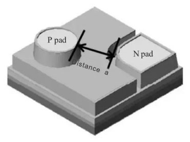
The structure of the LED blue-green chip
It can be seen from picture, as the size is reduced, the pads of the P electrode and the N electrode are also reduced, and the reduction of the electrode pad directly affects the quality of the bonding wire, and it is easy to cause the gold ball to detach or even the electrode itself to detach during the packaging process and the use process, eventually lead invalid. At the same time, the distance a between the two pads will also shrink, which will cause the current density at the electrode to increase excessively, and the current will locally accumulate at the electrode, and the unevenly distributed current seriously affects the performance of chip, causing the chip to have problems such as a local temperature excessive height, uneven brightness, easy leakage, drop of electrodes, and even low luminous efficiency ultimately lead to reduced reliability of the LED display.
3. Bond wire
The bonding wire is one of the key materials of the LED package. Its function is to realize the electrical connection between the chip and the pin, and to play the role of current and output of the chip and the outside. Common bonding wires for LED device packages include gold wires, copper wires, palladium-plated copper wires, and alloy wires.
(1) Gold wire. Gold wire used the most widely,process the most mature , but expensive, resulting in high packaging cost of LED.
(2) Copper wire. Copper wire instead of gold wire has the advantages of low cost, good heat dissipation effect, and slow growth of intermetallic compounds during wire bonding. The disadvantage is that copper is easily oxidized, has high hardness and high strain strength. Especially in the heating environment of the bonding copper ball burning process, the copper surface is easily oxidized, and the formed oxide film reduces the bonding property of the copper wire, which puts higher requirements on the process control in the actual production process.
(3) Palladium-plated copper wire.In order to prevent oxidation of copper wires, palladium-bonded copper wires are gradually attracting attention from the encapsulation industry. Palladium-bonded copper wire has the advantages of high mechanical strength, moderate hardness, good soldering and ball bonding,etc.It is very suitable for high-density, multi-pin integrated circuit packages.
4. Glue
At present, the glue of the LED display device encapsulation mainly includes epoxy resin and silicone.
(1) Epoxy resin. Epoxy resin is easy to age and be wet, and has poor heat resistance. It is easy to change color under short-wave illumination and high temperature. It has certain toxicity in colloidal state.Thermal stress and LED do not match very well, which will affect the reliability and lifetime of LED.
(2) Silicone. Compared with epoxy resin, silicone has high cost performance, excellent insulation, dielectric properties and adhesion. But the disadvantage is that the air tightness is poor and it is easy to absorb moisture.Therefore, it is rarely used in encapsulation applications for LED display devices.
In addition,high-quality LED displays place special demands on the display.Some encapsulation plants use additives to improve the stress of the glue while achieving a matte effect.