+86 135 3053 5995
sales@mydled.comWe use our own and third-party cookies to ensure the proper functioning of the web portal and its complements, perform navigation analysis and show multimedia content. If you continue browsing, you accept the use of this technology. For more information please see our Cookies Policy. Learn more
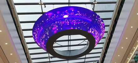
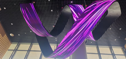
With the development of led technology, from large-spacing outdoor products to indoor led display screens for close viewing, indoor applications are becoming more and more common. Especially under the current rapid development of smart cities and the security industry, as well as the current development of digital enterprises and the digital age, the demand for indoor display hardware continues to increase.
1) The evolution history of indoor display products
Since 2015, the localization rate of MOCVD has increased rapidly, the production capacity of LED chips has been released rapidly, and the decline in chip prices has effectively reduced the price of LED lamp beads. The maturity of technology makes the package size of lamp beads smaller and smaller, and promotes the development of the industry.
The categories of small pixel pitch leds have increased, and they have begun to compete with DLP and LCD in the indoor display market. According to the data on the scale of the global led display market, from 2018 to 2022, the performance advantages of small pixel pitch led display products will be obvious, forming a trend of replacing traditional LCD and DLP technologies.
2) Customer industry distribution of small pixel pitch led display
In recent years, small pixel pitch LEDs have achieved rapid development, but due to cost and technical issues, they are currently mainly used in professional display fields. These industries are not sensitive to product prices, but require relatively high display quality, so they quickly occupy the market in the field of special displays.
3) The development of small pixel pitch LEDs from the dedicated display market to the commercial and civilian markets
After 2018, as the technology matures and costs decrease, small pixel pitch LEDs will usher in an explosion in the commercial display market such as conference rooms, education, shopping malls, and movie theaters. The demand for high-end hd pixel pitch LEDs in overseas markets is accelerating. Seven of the world's top eight led manufacturers are from China, and the top eight manufacturers account for 50.2% of the global market share.

4) Analysis of small pixel pitch led packaging technology
SMD is the abbreviation for surface mount device. The bare chip is fixed on the bracket, and the electrical connection is made between the positive and negative electrodes through metal wires, and the epoxy resin is used for protection to make SMD LED lamp beads. After soldering the led lamp beads and the PCB through reflow soldering to form the led module, the led module is installed on the fixed cabinet, and the power supply, control card and wire are added to form the finished led display screen.
Compared with other packaging forms, SMD packaged products have more advantages than disadvantages, and are in line with the characteristics of domestic market demand (decision-making, procurement, and use). They are also the mainstream products in the current industry and can quickly receive service responses.

The COB process is to directly adhere the LED chip to the PCB with conductive or non-conductive glue, and wire bonding to achieve electrical connection (positive mounting process) or using chip flip-chip technology (without metal wires) to directly connect the positive and negative electrodes of the lamp beads. PCB connection (flip-chip technology), and finally the led module is formed, and then the led module is installed on the fixed cabinet, and the power supply, control card and wire are added to form the finished led display.
The advantages of COB technology are that it simplifies the production process, reduces product costs, and reduces power consumption, so the display surface temperature is reduced, and the contrast ratio is greatly improved. The disadvantage is that reliability faces greater challenges, difficult to repair lights, and it is difficult to achieve consistency in brightness, color, and ink color.
IMD integrates N groups of RGB lamp beads into a small unit to form a lamp bead. Main technical route: Common Yang 4 in 1, Common Yin 2 in 1, Common Yin 4 in 1, Common Yin 6 in 1, etc. Its advantage lies in the advantages of integrated packaging, the lamp bead size is larger, the surface mounting is easier, smaller pixel pitches can be achieved, and maintenance difficulties are reduced. The disadvantage is that the current industrial chain is not perfect, the price is high, the reliability is facing greater challenges, the maintenance is inconvenient, and the brightness, color, and ink consistency have not been resolved, and further improvement is needed.
Micro LED is to transfer a huge amount of addressing from traditional LED arrays and miniaturization to the circuit substrate to form ultra-fine-pitch LEDs. The length of the millimeter-level LED is further reduced to the micron level to achieve ultra-high pixels and ultra-high resolution. In theory, it can be adapted to various screen sizes. At present, the key technology of Micro LED lies in the breakthrough of miniaturization process technology and mass transfer technology. Secondly, thin film transfer technology can break through the size limit to complete batch transfer, which is expected to reduce costs.
GOB is a technology for covering the entire surface of surface mount modules. It encapsulates a layer of transparent colloid on the surface of traditional SMD small-pitch modules to solve the problem of strong shape and protection. In essence, it is still SMD small-pitch products. Its advantage lies in reducing the dead-light rate, increasing the anti-collision strength and surface protection of the lamp beads. The disadvantage is that it is difficult to repair the lamp, the deformation of the module caused by the colloidal stress, reflection, partial degumming, colloidal discoloration, and the difficulty of repairing the virtual welding.
AOB is a technology for covering the bottom of surface mount modules. It also encapsulates a semi-layer transparent colloid in the gap between the lamp beads of the traditional SMD small-pitch module to solve the problem of protection. In essence, it is still a small-pitch SMD product. There are limitations and potential risks. For example, it is difficult to achieve a pitch below P1.25, only TOP lamp beads can be used, and potential problems with the surface mount process still exist.
COG packaging, the chip is directly bound to the glass through a conductive adhesive. The advantage is that the volume and weight of the display panel are greatly reduced, and the mass production is easy. However, there are certain limitations and potential risks. For example, because the glass substrate is limited in size, it is suitable for small-area applications and temporarily unsuitable for large-area splicing.
+86 135 3053 5995
+86 400 888 7260
No.9, The Third Industrial Zone of Nangang, Tangtou, Shiyan, Bao'an District, Shenzhen, China
Copyright © 2008 - 2028 Shenzhen Meiyad Optoelectronics Co., Ltd. Sitemap
share it: